Your Cart is Empty
Customer Testimonials
-
"Great customer service. The folks at Novedge were super helpful in navigating a somewhat complicated order including software upgrades and serial numbers in various stages of inactivity. They were friendly and helpful throughout the process.."
Ruben Ruckmark
"Quick & very helpful. We have been using Novedge for years and are very happy with their quick service when we need to make a purchase and excellent support resolving any issues."
Will Woodson
"Scott is the best. He reminds me about subscriptions dates, guides me in the correct direction for updates. He always responds promptly to me. He is literally the reason I continue to work with Novedge and will do so in the future."
Edward Mchugh
"Calvin Lok is “the man”. After my purchase of Sketchup 2021, he called me and provided step-by-step instructions to ease me through difficulties I was having with the setup of my new software."
Mike Borzage
Design Software History: Pioneering the Future: The Evolution of Design Software in the Semiconductor Industry
August 20, 2024 3 min read


Introduction to Design Software in the Semiconductor Industry
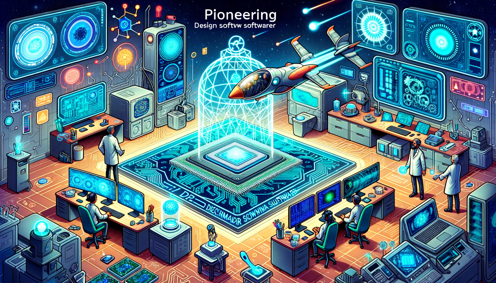
The semiconductor industry is a cornerstone of modern technology, providing the essential components that power everything from smartphones to supercomputers. At the heart of this industry lies **design software**, a critical enabler of innovation and efficiency. Design software encompasses a wide array of tools and platforms that assist engineers in creating, testing, and optimizing semiconductor devices.
Historically, the path to efficient semiconductor design was fraught with challenges. Initial efforts were heavily manual, relying on human precision and time-consuming methods. The evolution toward automation marked a significant transformation, paving the way for the sophisticated Electronic Design Automation (EDA) tools we see today.
Early Pioneers and Milestones
Seminal Companies and Innovators
The 1960s were a transformative period for semiconductor design, marked by pioneering efforts from companies like **Fairchild Semiconductor** and **Texas Instruments**. These firms made significant strides in developing the foundational technologies that would shape the industry. Key figures such as **Jack Kilby** of Texas Instruments and **Robert Noyce** of Fairchild Semiconductor were instrumental in advancing early semiconductor technology.
At the same time, **Bell Labs** emerged as a hub of innovation, contributing to the development of integrated circuits. Engineers at Bell Labs, including experts like Kilby and Noyce, were at the forefront of overcoming the limitations of discrete component designs.
Key Developments
One of the pivotal innovations in the history of semiconductor design software was the introduction of **SPICE (Simulation Program with Integrated Circuit Emphasis)** at UC Berkeley. Developed in the 1970s, SPICE revolutionized the way engineers simulate and analyze the behavior of electronic circuits, making it an indispensable tool in the design process.
The advent of the first **Electronic Design Automation (EDA)** tools marked another significant milestone. These tools automated many of the labor-intensive aspects of semiconductor design, significantly enhancing productivity and accuracy.
Evolution of EDA Software
Technological Advancements
The transition from manual drafting to **computer-aided design (CAD)** represented a monumental leap in the efficiency and precision of semiconductor design. Early CAD systems provided a digital platform for drafting and schematic capture, laying the groundwork for more advanced EDA tools.
The development of hardware description languages such as **Verilog** and **VHDL** in the 1980s and 1990s further advanced the field. These languages allowed engineers to describe the behavior and structure of electronic systems in a high-level, human-readable format, facilitating more complex designs and simulations.
Another critical advancement was the introduction of **RTL (Register Transfer Level) synthesis**, which enabled the automatic conversion of high-level hardware descriptions into gate-level implementations. This development streamlined the design process, reducing the time and effort required to bring new semiconductor devices to market.
Major Players and Software
Several companies have been pivotal in the evolution of EDA software. **Cadence Design Systems**, **Synopsys**, and **Mentor Graphics** are among the most influential, each contributing a range of innovative tools and platforms. For example, Cadence's **Virtuoso** platform has become a standard in the industry for analog and mixed-signal design, while Synopsys' **Design Compiler** is renowned for its capabilities in logic synthesis and optimization.
These companies have continually pushed the boundaries of what is possible with EDA software, integrating new technologies and methodologies to address the ever-growing complexity of semiconductor designs.
Current Trends and Future Directions
Modern Innovations
In recent years, the integration of **AI and machine learning** has begun to transform design software. These technologies offer powerful new capabilities for optimizing designs and predicting performance, significantly enhancing the efficiency and effectiveness of the design process.
Another emerging trend is the shift toward **cloud-based EDA tools**. These platforms offer scalable, on-demand resources, enabling engineers to handle larger and more complex designs without the need for significant upfront investment in hardware.
Challenges and Opportunities
As the semiconductor industry continues to push the boundaries of **Moore's Law**, new challenges emerge. Addressing the complexities of designing at ever-smaller scales requires increasingly sophisticated tools and methodologies.
At the same time, emerging technologies such as **quantum computing** and the **Internet of Things (IoT)** present new opportunities and demands. Design software must evolve to meet these needs, incorporating new paradigms and capabilities to support the next generation of semiconductor devices.
Vision for the Future
The future of EDA software holds significant promise. As tools continue to advance, their impact on the semiconductor industry will only grow, driving innovation and enabling new breakthroughs. The potential for **advanced EDA tools** to transform the industry is immense, offering new ways to tackle the challenges of modern semiconductor design and unlock new levels of performance and efficiency.
Looking ahead, we can expect ongoing innovations in design software to play a critical role in the continued growth and evolution of the semiconductor landscape, shaping the future of technology in profound and exciting ways.
Also in Design News

Rhino 3D Tip: Rhino Material Optimization: Nesting, Lightweighting, and Cut-Length Reduction
December 31, 2025 2 min read
Read More
Design Software History: Constraint Solving in CAD: From Sketchpad to Modern Parametric Engines
December 31, 2025 12 min read
Read More
Intent-Aware Scan-to-BRep: Integrating LiDAR Point Clouds into Solid Modeling Pipelines
December 31, 2025 12 min read
Read MoreSubscribe
Sign up to get the latest on sales, new releases and more …


