
Your Cart is Empty


Design Software History: From Tape to Terminals: Evolution of PCB Design Software, Routing Algorithms, and Manufacturing Data (1960s–Present)
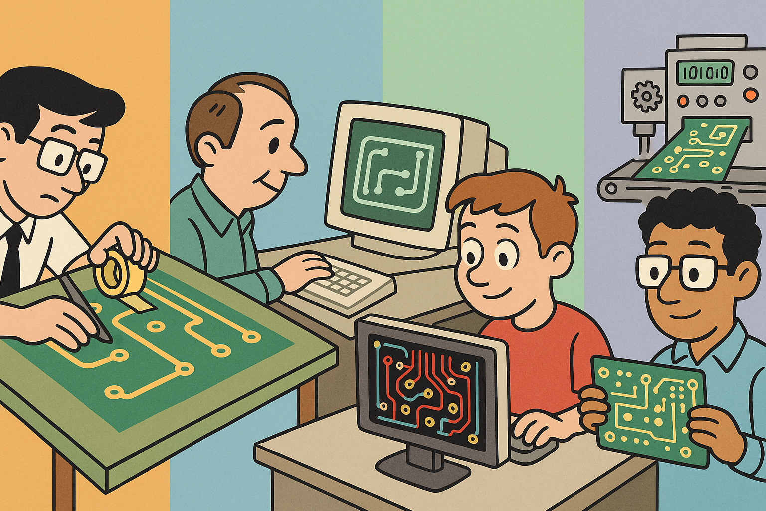


From Tape to Terminals: Early PCB Design and Foundational Algorithms (1960s–1980s)
Manual era and photoplotting
Printed circuit board work in the 1960s and 1970s began as a tactile craft rooted in materials and camera optics rather than in bits and bytes. Layout technicians composed routing by hand with Bishop Graphics adhesive tape on translucent mylar, trimming curves and corners with scalpels, and stacking Rubylith masks to define copper, solder mask, and silkscreen layers. The physicality mattered: line widths were constrained by tape sizes, and registration across layers depended on careful alignment pins and seasoned eyes. Once the artwork was complete, it was transferred to film through step-and-repeat cameras and eventually to copper via photoresist processes. This pipeline was accurate enough for the era’s component sizes yet inherently slow, and every edit meant peeling tape, replacing overlays, and re-shooting film. It also taught an important lesson that still holds: manufacturable geometry is as much about representation as it is about intent.
Mechanization arrived through the ingenuity of H. Joseph Gerber, whose photoplotters transformed vector commands into precisely imaged apertures on film. The plotting language that emerged—RS‑274D “Gerber”—codified aperture selections and moves, letting layout data be transferred to fabrication without the artwork’s physical bulk. Parallel to copper imaging, drilling data standardized around Excellon formats, where drill hits and tool tables could drive numerically controlled machines. But the early Gerber flavor separated shape data from aperture libraries, creating room for interpretation errors at the cam station. Typical production bundles contained: Gerber films, Excellon drill files, and reams of written notes explaining layer order, solder mask expansions, and plating assumptions. The practical consequence was a latent miscommunication risk that only became more critical as minimum features shrank and layer counts rose.
First ECAD systems and companies
By the late 1970s and early 1980s, minicomputers and workstations made it possible to draw layouts interactively rather than with tape. Early innovators included Racal‑Redac in the UK and Zuken in Japan (founded 1976), both targeting professional bureaus and OEMs who could afford dedicated hardware. In the United States, the “DMV” trio—Daisy Systems, Valid Logic, and Mentor Graphics—defined the workstation-era ECAD ambition: couple schematic capture, placement, routing, and verification into cohesive systems. Mentor Graphics, co‑founded in 1981 by Tom Bruggere, Gerry Langeler, and Dave Moffenbeier, capitalized on high-resolution graphics terminals and UNIX workstations to speed daily layout cycles and add logic-driven connectivity checks unthinkable on drafting tables.
Democratization accelerated as the IBM PC spread through engineering departments. PADS appeared in the mid‑1980s as a cost-effective tool that made professional PCB design viable on desktop machines. OrCAD (1985) popularized schematic capture on DOS and later Windows, and in Australia Nick Martin launched Protel—eventually Altium—with a mission to place layout and capture in a single, accessible environment. The PC not only cut costs; it changed expectations about iteration speed, library management, and revision control. Engineers could make changes themselves rather than sending requests to a centralized drafting pool. Still, data interchange remained riddled with ambiguity, and compute-limited autorouters hewed to simple grids. The stage was set for algorithms and data standards to mature together, so software could bridge the widening gap between design intent and build-ready output.
Routing breakthroughs that set the stage
Routing automation pivoted on algorithmic advances that began in academia and migrated into commercial tools. The foundational maze router, Lee’s algorithm (1961), treats the board as a grid and performs breadth‑first search, guaranteeing the shortest path if one exists. While robust, its wavefront expansion is computationally expensive. Hadlock’s algorithm (1977) introduced a detour-based heuristic, reducing expansions by favoring paths that minimally deviate from Manhattan distance, improving runtime on realistic boards. In parallel, researchers explored channel routing and area routing, developing compaction and via minimization strategies that influenced early workstation-era autorouters. The net effect was measurable: routing became more exhaustive, repeatable, and explainable, especially for two-layer and simple multilayer designs.
A second, equally important breakthrough was the representation shift from grid‑based geometry to shape‑based modeling. Grids simplify the search space but fight manufacturability when component pitches and trace widths misalign. Shape-based engines operate on polygons, arcs, and sophisticated clearance envelopes, enabling curved traces, teardrops, fillets, and pad entry conditions that better reflect how copper is etched and plated. This change allowed algorithms to reason about copper as continuous geometry, opening the door to push‑and‑shove interactions and post-route cleanups that minimized acid traps and lithographic artifacts. By the late 1980s, the ideas were in place; what remained was enough compute power and enough software engineering discipline to deliver these methods as reliable, commercial-grade features.
Data handoffs and ambiguity
Even as ECAD tools matured, manufacturing handoffs lagged. The canonical flow—netlist to layout to Gerber films and Excellon drill files—relied on external documents for the rest: plating instructions, layer stackups, impedance targets, fiducial requirements, and solder mask clearances. In practice, CAM operators reconstructed intent, sometimes inferring apertures, scaling assumptions, or polarity from context. With RS‑274D specifically, apertures were often referenced in a separate text file; mismatches between declared and used apertures caused missing shapes or unexpected outline widths. When a board passed but a variant failed, investigators might discover that a line labeled “keepout” had been interpreted as a mechanical outline, or that solder mask expansion defaults didn’t match the designer’s DFM assumptions.
The pain points clustered around ambiguity and loss of constraints, which were not encoded in the manufacturing data. Typical mitigation steps included:
- Embedding “readme” manufacturing notes that indexed each layer, described stackups, and set default expansions.
- Sending fabrication drawings with layer tables, drill charts, and impedance targets calculated offline.
- Maintaining “golden” aperture lists and instructing CAM to override ambiguous or missing definitions.
- Manual CAM reviews with marked-up film plots to verify polarity, film order, and tooling features.
These stopgaps worked when schedules and feature sizes allowed re-spins. As multilayer counts grew and fine‑pitch devices emerged, the ecosystem needed tighter integration, richer data formats, and routers that could solve for performance as well as topology. The 1990s would bring exactly that: integrated suites, shape‑based routing at scale, and standards tuned to eliminate interpretation gaps.
Integration, Standardization, and the Suite Era (1990s–2000s)
Unifying capture, simulation, and layout on PCs
The 1990s validated the PC as a professional engineering platform and fused once‑separate tasks into coherent design suites. OrCAD Capture replaced text‑centric schematics with intuitive drawing, while OrCAD Layout handled placement and routing on Windows. A pivotal moment arrived when MicroSim’s PSpice integrated into OrCAD; simulation became a first‑class citizen connected to netlists and libraries rather than a parallel activity. Protel, rebranded as Altium, pursued an integrated board‑level workflow emphasizing everyday usability, live DRC feedback, and library synchronization. PADS evolved into a Windows-native environment, refining constraint entry, part libraries, and fabrication outputs in a streamlined package.
This era’s shift was not just a convenience; it created feedback loops that improved design quality. Engineers iterated schematics, ran functional simulations, verified footprints, and pushed changes into layout without manual data transfers. The emerging idea of a “design database” unified logical and physical views, tying reference designators, parameter values, and footprints to a common source. Practical benefits included:
- Reduced errors from symbol/footprint mismatches, thanks to centralized libraries.
- Faster ECO cycles because changes in capture propagated accurately to layout.
- Early detection of shorts/opens through live connectivity checking.
- More consistent documentation, with BOMs, netlists, and drawings sourced from the same database.
By the decade’s end, teams expected a suite that spanned capture, simulation, layout, and output generation, establishing the baseline that modern platforms still build upon.
Enterprise-class platforms take shape
As product complexity grew, so did the need for enterprise-grade configuration control, constraints, and multi‑user collaboration. Cadence Allegro emerged as a high-end platform capable of handling large designs, dense BGAs, and complex rulesets. Mentor Graphics delivered Board Station for established flows and later Expedition (which became Xpedition), emphasizing high‑capacity routing, constraint management, and design‑reuse features for global teams. In Japan and beyond, Zuken CR‑5000 offered robust libraries, hierarchical design, and manufacturing-aware checks, reflecting Zuken’s deep ties to large OEMs and their supply chains.
These enterprise tools converged on a similar set of capabilities: hierarchical constraints, centralized part and footprint governance, data management with versioned libraries, and collaboration assets like design partitioning or concurrent editing. Another differentiator was scalability—how well the database and UI maintained performance with tens of thousands of nets and components. Over time, vendor ecosystems matured around these platforms:
- Managed libraries and vaults that enforced standards and obsolescence policies.
- Tight integrations with PLM/ERP systems to connect ECAD data to procurement and compliance.
- Portal interfaces that allowed fabricators and assemblers to annotate DFM issues within design context.
The result was a professional landscape with clear tiers: accessible PC suites for mainstream boards and enterprise systems for high‑density, multi‑disciplinary programs where governance and scalability were as important as routing performance.
Autorouting matures and goes commercial
The period’s most dramatic leap was the commercialization of truly capable shape‑based routing. SPECCTRA, created by Cooper & Chyan Technology and acquired by Cadence in 1997, set the benchmark with obstacle‑aware geometry, rip‑up-and‑retry strategies, and routability for dense BGA breakouts. Unlike grid routers, SPECCTRA manipulated polygonal data and enforced dynamic clearances, bringing earlier research ideals to production reality. Other vendors followed suit, and the language of push‑and‑shove interactive routing entered day‑to‑day practice, letting designers route by hand with algorithmic assistance that moved neighbors out of the way while maintaining rules.
Commercial success hinged on a balanced workflow: use an auto-router to complete the bulk of connections under constraints, then refine interactively with shove-and-slide operations, fanout optimizations, and post‑route cleanup. Typical benefits included:
- Shorter routing cycles for large designs due to automated escape routing and layer optimization.
- Fewer DRC violations thanks to on‑the‑fly obstacle avoidance and teardrop/fillet capabilities.
- Better via economy through cost functions that penalized unnecessary layer changes.
Crucially, router engines became embedded in the daily UI, not relegated to batch runs. The tight interplay between rules, routing, and immediate visual feedback trained a generation of designers to think algorithmically about constraints—foreshadowing the constraint-managed paradigms that followed in the 2010s.
Manufacturing data and DFM evolve
During this same window, manufacturing output formats evolved to remove ambiguity and empower DFM feedback. Gerber RS‑274X embedded apertures directly into the files, an advance stewarded by Ucamco that eliminated a common source of misunderstandings. Meanwhile, Valor introduced ODB++, a richer container capturing layers, drill, netlists, components, and attributes in a single cohesive dataset. ODB++’s adoption accelerated when Valor’s DFM tools could ingest the data and present actionable findings back to ECAD teams; later, Valor became part of Mentor Graphics and now Siemens EDA. In parallel, industry stakeholders championed IPC‑2581, derived from GenCAM, as an open, neutral alternative to increase vendor interoperability and break proprietary lock‑ins.
Extensible manufacturing data unlocked new workflows:
- Automated stackup verification and drill checks using layer/material metadata.
- Netlist compare at the CAM station to catch etch or data errors before costly steps.
- Round‑trip DFM where fabrication constraints—minimum annular ring, resin dams, solder mask webs—could be validated in design, not just post‑tapeout.
With clearer semantics and fewer side documents, designers could ship “correct by construction” packages. This evolution, coupled with maturing signal integrity workflows, primed the industry for the next decade’s central theme: constraints as first‑class design objects tightly integrated with simulation and 3D context.
Signal/power integrity enters mainstream PCB flows
As edge rates climbed and fine‑pitch devices proliferated, Maxwell’s equations moved from theory to practical necessity. HyperLynx (Mentor) made signal integrity approachable, providing pre‑ and post‑layout analyses for reflections, crosstalk, and timing. Sigrity (later acquired by Cadence) specialized in high‑end SI/PI extraction, integrating with Allegro to analyze simultaneous switching noise, return current continuity, and power plane resonances. Ansys SIwave and HFSS brought full‑wave EM accuracy to critical interconnects, connectors, and complex power distribution networks. The common thread was tighter loop closure: extract from layout, analyze, and feed constraints back into the design database.
Another mainstream milestone was professional stackup planning. Companies like Polar Instruments made impedance modeling and field-solver‑backed calculators accessible, aligning dielectric choices, copper weights, and trace widths to hit target impedances reliably. Designers began to encode differential pair rules, length matching targets, and return path constraints as hard requirements rather than guidelines. By the early 2000s, high‑speed design ceased to be a niche specialty; it became a standard capability in serious ECAD suites, anchored by workflows that bound analysis results to enforceable rules in layout.
Constraint-Driven, Model-Based Co-Design (2010s–present)
From DRC to constraint managers
The 2010s reframed PCB design around a central thesis: encode design intent as constraints and have tools maintain compliance continuously. Instead of simple DRC checks (clearance, width, and overlap), modern platforms maintain hierarchical, object-aware rule sets. Designers specify impedance targets, differential pair coupling, length/delay/skew budgets, via types (through, blind, buried, microvia), creepage distances for high voltage, and region‑based constraints for zones like BGA breakout fields. Constraint managers express these as templates tied to net classes, physical rooms, or component groups and provide live compliance indicators during placement and routing.
Three operational shifts define this era:
- Live rule checking that prevents violations as the cursor moves, with visual overlays and route guides that reflect target impedance or length budgets.
- Template reuse so that once a DDR4 channel is validated, its topology, constraints, and length match groups can be reapplied to new designs or variants.
- Object awareness where pads, vias, shapes, and 3D models carry attributes (e.g., stackup layer, dielectric, plating) that drive both DFM and SI/PI behavior.
Under the hood, engines blend geometric reasoning with timing and EM heuristics. A modern router not only avoids overlaps; it tunes trace widths for impedance in designated layers, respects neck‑down rules near pads, and applies dynamic phase tuning for differential pairs. Constraints have become executable specifications—goals that the tool actively helps achieve rather than fences that flag violations after the fact.
High-speed, HDI, and mechanical context drive 3D workflows
Contemporary interconnects—DDRx, PCIe, USB 3.x/4, and multi‑gigabit SerDes—tighten tolerances on length, skew, and return path integrity, making 3D context non‑negotiable. HDI techniques (microvias, blind/buried vias, via‑in‑pad) complicate drill planning, resin flow, and reliability analysis, especially across multiple lamination cycles. Rigid‑flex designs bring bend radii, dynamic flex region constraints, coverlay clearances, and adhesive flow into the ECAD domain—phenomena that 2D checks cannot capture. As a result, 3D design evolved from visualization to verification and guidance.
ECAD‑MCAD co‑design matured through STEP exchanges and the EDMD/IDX protocol, which supports incremental updates—“propose/accept” changes to keep enclosures, keepouts, and component heights in sync. In practice, designers analyze:
- 3D clearances between components, shields, and enclosures to avoid interference and to control EMI coupling paths.
- Layer‑specific impedance feasibility within thickness and dielectric tolerances provided by fabricators.
- Via transition strategies that minimize stub-induced resonances (e.g., backdrilling decisions tied to stackup data).
The shift to 3D also aids manufacturing: accurate models of solder mask dams, paste apertures, and via tenting strategies feed assembly simulations and DFM checks. Ultimately, performance, reliability, and mechanical feasibility converge in a single interactive model, enabling confident signoff before any copper is etched.
In‑design verification and fab collaboration
The boundary between design and verification continues to dissolve. Field‑solver‑assisted engines estimate impedance and coupling as traces are drawn, not weeks later. Real‑time SI/PI/EMI checks flag return path discontinuities, reference plane splits, and cavity resonances likely to trigger emissions issues. Instead of exporting snapshots to external tools, designers can run incremental extractions directly on the editable database, with sensitivity analyses that show how small geometry changes perturb timing or impedance targets.
Manufacturability has become “by construction.” Rule‑deck‑based DFM—often sourced from fabricators—validates annular rings, resin fills, solder mask webs, and drill aspect ratios inside the ECAD environment. Stackup co‑development workflows let fabricators propose material sets, copper roughness models, and press‑fit hole tolerances that are accepted inline, updating impedance predictions as materials change. Outcome-oriented practices include:
- Early drill strategy signoff for HDI (sequential build steps, cap/skip microvia rules, backdrill coverage).
- Automated teardrop and fillet insertion tuned to fabricator etch compensation and AOI recognition.
- Assembly-aware checks for tombstoning risk, paste transfer efficiency, and package‑specific keepouts.
This loop shortens cycles and reduces surprises, aligning ECAD decisions with real manufacturing windows and yield expectations.
Tool and ecosystem milestones
The modern landscape is a tapestry of integrated platforms and open initiatives. Cadence binds Allegro layout with Sigrity analysis, while Allegro’s router inherits technology from the SPECCTRA lineage, blending shape‑based algorithms with interactive tuning. Siemens EDA (Mentor) offers Xpedition paired with HyperLynx, and anchors manufacturing with Valor DFM and ODB++ data flows. Zuken CR‑8000 extends from multi‑board partitioning to system‑level design management, reflecting the trend toward product‑centric, multi‑PCB assemblies.
Altium Designer emphasizes a unified environment—schematics, layout, rules, 3D, and documentation—with features such as ActiveRoute for guided automation and supply‑chain context via Octopart integration. On the open-source front, KiCad, initiated by Jean‑Pierre Charras, has expanded remarkably with contributions from CERN, including a push‑and‑shove router, differential pair handling, and length tuning that rival commercial tools for many classes of designs. The broader ecosystem now includes:
- Cloud-backed libraries and rule repositories that encode corporate standards and compliance requirements.
- API-driven integrations to PLM, requirements management, and simulation platforms.
- Continuous design “linting” that tracks constraints, SI/PI risks, and DFM issues across revisions.
The overall direction is clear: constraints and models form the backbone, routers and solvers provide the muscle, and collaborative data services tie the process together from concept to first article.
Conclusion
From manual artistry to executable intent
Across six decades, PCB design has shifted from craft to computation, from tape and Rubylith to constraint‑solved, model‑based engineering. Early years taught the persistent lesson that representation governs manufacturability—what you can express cleanly in data, you can build reliably in copper. The 1990s to 2000s fused capture, layout, and simulation into suites and elevated shape‑based routing—epitomized by SPECCTRA—to production normalcy. Manufacturing formats evolved from RS‑274D ambiguity to RS‑274X embeddings and richer containers like ODB++ and IPC‑2581, tightening the feedback loop with CAM and fabrication. In the 2010s and beyond, platforms transformed rules into living entities: impedance, skew, and via rules are enforced as you draw, and multi‑physics checks guide decisions within an integrated 3D context.
Several inflection points stand out as accelerants:
- Gerber standardization that unlocked reliable photoplotting and digital-to-optical fidelity.
- Shape‑based autorouting that made dense, manufacturable layouts tractable and interactive.
- Integrated SI/PI workflows that turned EM realities into everyday design constraints.
- Neutral manufacturing data—IPC‑2581 and ODB++—that reduced interpretation risk and enabled DFM by construction.
The consequence is a discipline where intent is executable: databases carry semantics about materials, fields, and manufacturability, and tools act as partners in maintaining that intent from schematic to shipment.
Vectors that will shape the next decade
The near future will consolidate this progress and push into new territory where automation reasons about specifications, supply chains, and compliance holistically. Expect to see:
- AI‑assisted placement/routing that proposes floorplans, derives constraints from datasheets and interface standards, and predicts congestion and SI pitfalls before they materialize.
- Rule synthesis from formal requirements: transform DDR timing constraints, creepage clearances, or EMI limits into enforceable rule decks automatically.
- Cloud‑native collaboration with live supply‑chain intelligence—stock, lifecycle, and compliance—embedded into part choice and risk analysis.
- Deeper ECAD‑MCAD‑CAE convergence where multi‑physics closure (thermal, structural, EM) is achieved iteratively with fab‑validated stackups that meet impedance and reliability goals by construction.
The enduring lesson is that progress compounds when algorithms, standards, and ecosystems advance together. PCB design ceased to be “drawing wires” when routers learned geometry, when formats carried semantics, and when solvers moved in‑design. The next leap will be intent captured at the level of behavior and compliance, executed by tools that understand manufacturing as deeply as they understand math. In that world, the most valuable artifact is not a set of files; it is an executable, traceable expression of engineering intent that travels intact from concept to copper.
Also in Design News